03 — CPU Architecture

03 — CPU Architecture
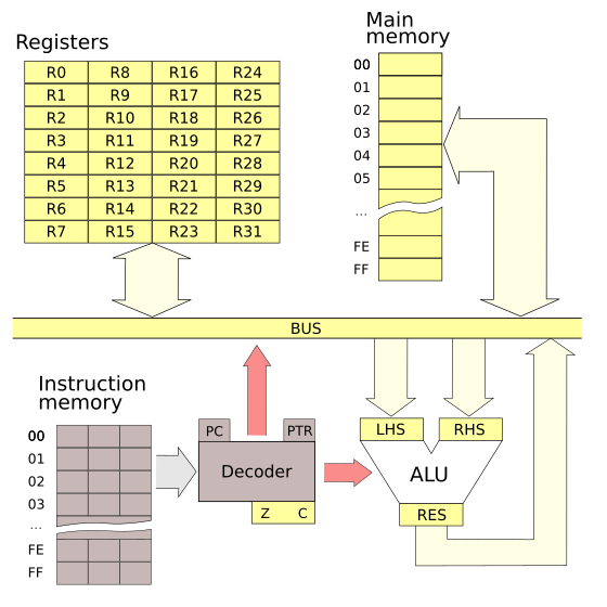
This video showed the major components common to all computers, and
how the instruction decoder directs the other components to carry out
each instruction step by step, before moving on to the next
instruction. It likened the decoder to "the conductor of an
orchestra".
Knowing the particular steps is not terribly important. Neither is knowing of the existence of an ALU. Even CPU registers are only of interest to assembly language programmers. Here are what I think are the key facts in this video:
In assembly language, you have to keep order. When using higher level languages, they have great features to help — arrays, structures, data typing — but everything is still being stored in that blob, and poor programming can still bite you. You may think your typing is being saved into a string, but you've typed too much, gone past its end, and now your keystrokes are overwriting somebody's bank balance (or whatever).
The diagram has something labelled "BUS", described in the video as "a set of wires". More correctly, it's the data bus. Computers also have an address bus. It's another set of wires, the number of wires being the number of bits in the address. The decoder uses the address bus to tell a particular memory cell to read or write its value on the data bus.
A brief look at the advantages of a Harvard architecture over a von Neumann architecture (as used in PCs).
more secure
Many PC viruses write a few bytes somewhere in RAM and get the CPU to
jump there. Machine taken over. More recent processors have extra
memory protection to prevent this sort of behaviour.
higher performance
The two different blocks of memory can be accessed at the same
time e.g. fetch the next instruction while writing out the data from
the previous instruction. Again, von Neumann architectures have
added instruction and data caches and instruction pipelines which
pretty much nullifies this Harvard advantage.
doubles the address space
Instructions don't use up main memory address space and vice versa.
This is the reason ArdEx has a Harvard architecture. We get 256 main
memory cells and 256 instruction slots. Things would have been very
tight otherwise.
 ArdEx has separate main memory and instruction memory, and each has an
8-bit address space. That gives 256 instruction slots to play
with, and 256 main memory addresses.
ArdEx has separate main memory and instruction memory, and each has an
8-bit address space. That gives 256 instruction slots to play
with, and 256 main memory addresses.
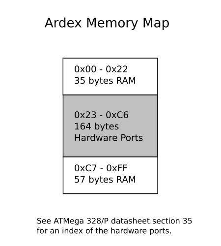
Unfortunately, the main memory space is shared with the ATmega328/P I/O ports. I/O ports are "magical" locations in the memory address space. The computer monitors the address bus and, when it notices an address that matches an I/O port address, it intercepts the signal and passes it to whatever fancy gadget has been given that address. This is called memory mapped I/O, and it's very common.
The diagram shows that the ATmega intercepts addresses in the 0x23 to 0xC6 range. You can browse the Register Summary section of the ATmega datasheet if you want to check them out. You'll see PORTB at 0x25, as mentioned in the video.
With all those addresses used up for I/O, we only have 92 bytes of RAM available for ArdEx to use. While the video said it wasn't even in one block, in a way it is. Say you needed a 64-byte chunk for some purpose, you could start at 0xC7 and, because addresses wrap around like an odometer, the last byte of your chunk would be at 0x06. A little strange, but no reason why not.
The usual alternative to memory mapped I/O is I/O mapped I/O. It's not a very inspiring name, but it means that there is a dedicated I/O subsystem. This can have a performance advantage since the CPU can continue operations while the I/O system does its work, but there are two drawbacks. Firstly, it's yet another bus, more wires, more pins. Secondly, it requires dedicated I/O instructions in the CPU's instruction set.
Nearly all processors include a system stack. As the name suggests, it works like stacking plates. The last item put on is always the next one to be taken off. A stack is also known as a LIFO. The system stack usually occupies ordinary memory and builds downwards.
ArdEx doesn't have a visible system stack. It was a trade-off; it would have been more powerful, but more complicated too. As a compromise, ArdEx has pre-decrement and post-increment register addressing modes which make it easy to create a stack.
Given how simple each instruction is, it's not a whole lot to learn, is it?
In the video, I said that manufacturers usually publish timing figures for processors' instruction sets. I haven't done this for ArdEx, but my measurements on an oscilloscope show instructions vary in duration beween 8 and 11 µs. For most purposes it's pretty safe to say they take 10 µs (with the exception of WAIT of course). But be warned, the timing isn't going to be very accurate.
Intel can no longer provide meaningful timing figures for their PC processors. For one thing, the instructions come to the decoder through a pipeline, and a pipeline manager examines the instructions, reordering them to maximise performance. For example, it might look at the next three instructions, notice that the first two access memory, and the third does an operation on a register not affected by the first two. Memory operations take several cycles, so the decoder puts the register operation in between the memory access operations. It gets executed "for free" during the memory access delay. What should Intel put for the cycle counts of these three instructions?
When you factor in the instruction pipeline along with data and instruction caching, it's enough to make your head spin. It's not worth worrying about. What has really happened is that Intel's people have pretty much taken on for themselves the low-level optimisations that used to be the programmer's problem.
Microcontrollers are much simpler of course, and typically have well defined timings for their instruction sets. While most have very useful built-in timers, it's sometimes best to use CPU cycle counts, typically to get short and accurate delays.
Programmers aren't out of a job yet.